
Where Stage 2 begins and ends
Stage 2 starts after the charger-controller stage has produced approximately 12.3V PPBUS_AON from the initial 5V USB-C input. U5200 then asserts P3V8AON_PWR_EN, also called EN_MVR in functional descriptions. This enable starts U5700 and creates PP3V8_AON.
The stage ends when the important always-on outputs and the first S2 outputs are present:
- PP3V8_AON from U5700
- PP1V8_AON, PP1V2_AON and PP3V3_AON from MPMU U8100
- PMU_CRASH_L high, confirming that the MPMU is not reporting a crash condition
- PP1V2_S2 from MPMU U8100
- PP5V_S2_MAIN from external regulator UC260 after an MPMU enable
- PMU_CLK32K_SOC from U8100
- PP0V72_S2_VDDLOW from SPMU U7700
The following Viper, Monaco and SoC awake-rail stage should not be diagnosed until these prerequisites are stable.
Stage 2 sequence overview
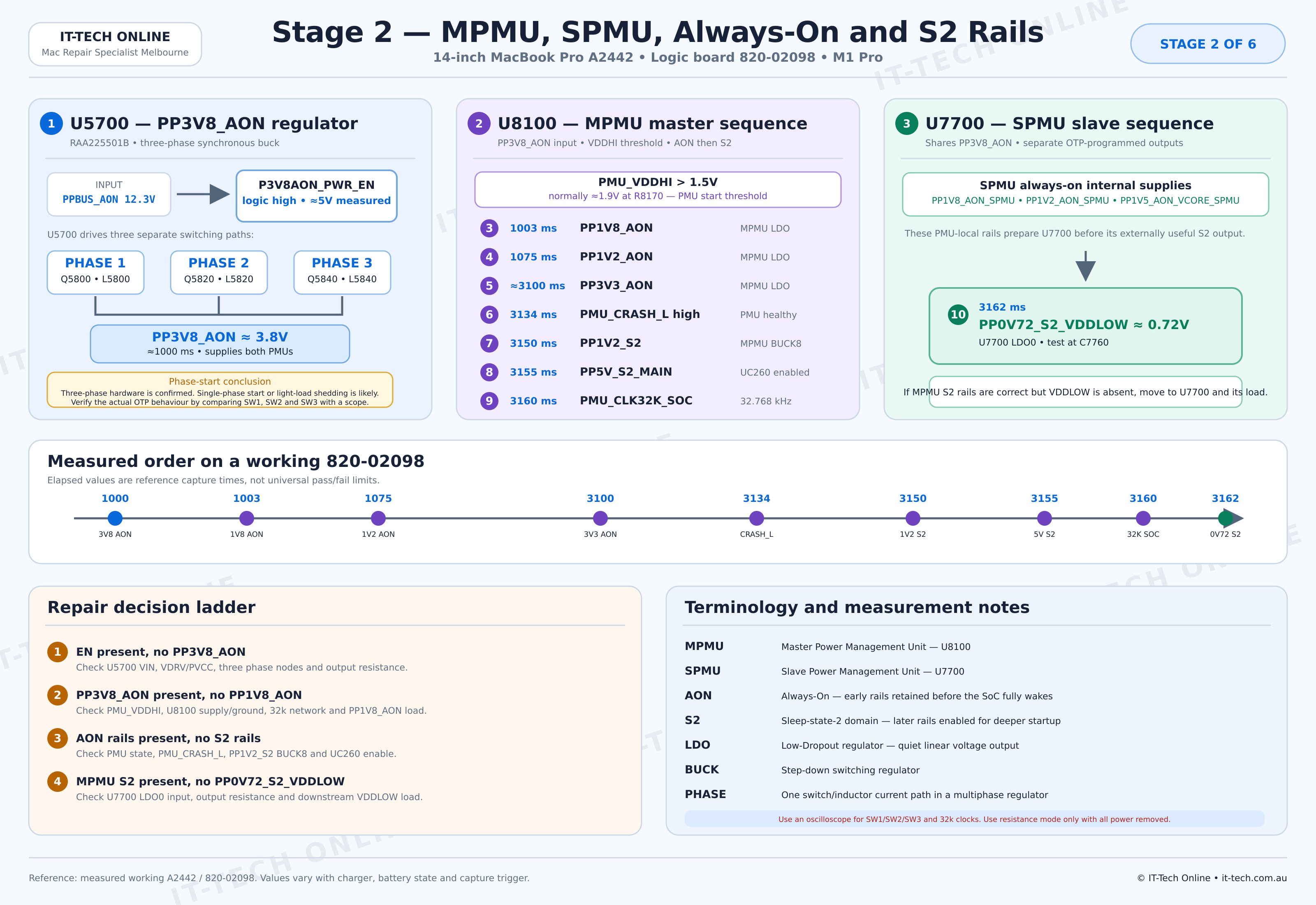
U5700 creates PP3V8_AON
U5700 is identified on the 820-02098 schematic as an RAA225501B three-phase voltage regulator. It is not a simple LDO. It is a high-current synchronous buck regulator with three independent driver and switching paths.
U5700 startup prerequisites
| Input or control | Expected condition | Purpose |
|---|---|---|
| PPBUS_AON | Approximately 12.3V during the initial boost stage | Main energy input for the 3.8V regulator |
| P3V8AON_PWR_EN | Logic high; approximately 5V in the working-board measurement | Enables U5700 |
| Internal LDO5 / PP5V_AON_P3V8AON | Approximately 5V after enable | Supplies the controller and initial gate-drive power |
| PVCC / VDRV | Gate-driver supply present | Allows the high-side and low-side power switches to operate |
| PP3V8_AON resistance | No short to ground | Allows soft start to complete without immediate over-current protection |
At the beginning of the sequence PP5V_S2_MAIN does not yet exist. U5700 therefore has an internal LDO5 path for its early gate-drive and control supply. After PP5V_S2_MAIN appears, the schematic permits the external 5V rail to supply VDRV as a lower-loss operating option.
The three U5700 power phases
The controller exposes three sets of high-side drive, low-side drive, bootstrap and switch-node pins:
- Phase 1: P3V8AON_DRVH1, P3V8AON_DRVL1 and P3V8AON_SW1, driving the Q5800 and L5800 path
- Phase 2: P3V8AON_DRVH2, P3V8AON_DRVL2 and P3V8AON_SW2, driving the Q5820 and L5820 path
- Phase 3: P3V8AON_DRVH3, P3V8AON_DRVL3 and P3V8AON_SW3, driving the Q5840 and L5840 path
The three inductor outputs join to form PP3V8_AON. Separate phase-current sensing allows U5700 to balance the load and protect the approximately 30A design. On the working capture PP3V8_AON reaches approximately 3.8V at about 1000ms.
Why PP3V8_AON is the hand-off point
PP3V8_AON is the power hand-off from the charger section into the PMU section. It supplies both U8100 MPMU and U7700 SPMU through their dedicated current-sense input branches. If PP3V8_AON is absent, neither PMU can complete its programmed output sequence.
This creates a strong diagnostic boundary:
- P3V8AON_PWR_EN low: remain in the U5200 ISL9240 stage.
- Enable high but PP3V8_AON missing: diagnose U5700, its three power stages, its drive supplies and the PP3V8_AON load.
- PP3V8_AON correct but PMU outputs missing: move to U8100/U7700 supply, reset, clock and load diagnosis.
MPMU U8100 output sequence
U8100 is the Master Power Management Unit. It provides the principal always-on rails, generates or controls multiple S2 and awake rails, distributes clock and reset signals, monitors analogue inputs and coordinates later power-state changes.
PMU_VDDHI starts the MPMU
PMU_VDDHI is derived from PPBUS_AON through the high-value input network around R8170. The working board measures more than 1.5V and normally approximately 1.9V at this point. U8100 requires this high-voltage supervisory input to start its buck and LDO outputs.
PP3V8_AON can therefore be present while U8100 remains inactive if PMU_VDDHI is missing or below its threshold. Check R8170, the VDDHI path and U8100 before blaming the output rails.
First MPMU always-on outputs
Once its startup conditions are satisfied, U8100 creates the first low-voltage rails in a programmed order:
| Approximate time | Output | Source | What it confirms |
|---|---|---|---|
| 1003ms | PP1V8_AON ≈1.8V | U8100 VLDO1V8 | The MPMU has begun its always-on LDO sequence |
| After PP1V8_AON | MPMU_XTAL2 32.768kHz | U8355 crystal/oscillator network | The MPMU timing reference is operating |
| 1075ms | PP1V2_AON ≈1.2V | U8100 VLDO1V2 | The 1.2V always-on logic domain is available |
| Approximately 3100ms | PP3V3_AON ≈3.3V | U8100 LDO output | The later always-on domain has been released |
| 3134ms | PMU_CRASH_L ≈1.2V high | U8100 status output | The PMU is not asserting a crash/restart condition |
The approximately two-second gap between PP1V2_AON and PP3V3_AON is present in this particular capture and should not automatically be interpreted as a stall. Diagnose by sequence order and rail stability, not by demanding identical timing on every board.
MPMU transition into S2 outputs
After the always-on logic is established, U8100 enables the first S2 rails:
- PP1V2_S2: approximately 1.2V at 3150ms, generated by MPMU BUCK8 and measurable around L8280.
- PP5V_S2_MAIN: approximately 5.1V at 3155ms. U8100 asserts P5VS2TPS_PWR_EN so external regulator UC260 creates this rail. It is controlled by the MPMU but not generated inside U8100.
- PMU_CLK32K_SOC: approximately 32.768kHz at 3160ms, distributed from U8100 toward the SoC/embedded-management clock domain.
This ownership distinction is important. If P5VS2TPS_PWR_EN is missing, diagnose the MPMU state. If the enable is present but PP5V_S2_MAIN is absent, diagnose UC260, its input/output components and the 5V S2 load.
SPMU U7700 output sequence
U7700 is the Slave Power Management Unit. “Slave” does not mean that it is a passive regulator controlled pin-by-pin by U8100. U7700 is a large programmable PMIC with its own buck converters, LDOs, GPIOs, monitoring and OTP-defined sequencing. It shares the system power-management architecture with the MPMU and supplies rails assigned to the second PMIC.
SPMU local always-on preparation
The SPMU receives PP3V8_AON through PP3V8_AON_SPMU_ISNS and develops PMU-local always-on supplies shown in the schematic, including PP1V8_AON_SPMU, PP1V2_AON_SPMU and PP1V5_AON_VCORE_SPMU. These local outputs prepare U7700 before its later S2 and awake rails are required.
The exact internal ordering of every SPMU-local rail is OTP controlled and is not fully represented by the working-board measurement table. For diagnosis, confirm PP3V8_AON at U7700 and then check the first externally useful SPMU milestone.
PP0V72_S2_VDDLOW
At approximately 3162ms, U7700 LDO0 creates PP0V72_S2_VDDLOW at about 0.72V. This occurs only a few milliseconds after the MPMU S2 outputs appear. It confirms that the SPMU has powered, accepted the platform state and released its low-voltage S2 output.
If PP1V2_S2 and PP5V_S2_MAIN are stable but PP0V72_S2_VDDLOW is absent:
- Power off and check the resistance of PP0V72_S2_VDDLOW to ground.
- Confirm PP3V8_AON reaches the SPMU input sense branch.
- Confirm the SPMU-local always-on supplies are not missing or shorted.
- Check the PP0V72 output capacitor and trace around C7760.
- Use current draw and thermal inspection to identify a shorted downstream load before replacing U7700.
Complete measured Stage 2 order
| Order | Approximate time | Signal | Expected value | Practical test point | Owner |
|---|---|---|---|---|---|
| 1 | 1000ms | PP3V8_AON | 3.8V | L5800 output side / rail capacitor | U5700 |
| 2 | Before PMU outputs | PMU_VDDHI | >1.5V; normally ≈1.9V | R8170 | U8100 prerequisite |
| 3 | 1003ms | PP1V8_AON | 1.8V | R8317 / rail capacitor | U8100 LDO |
| 4 | After PP1V8_AON | MPMU_XTAL2 | 32.768kHz | U8355 network | U8100 clock |
| 5 | 1075ms | PP1V2_AON | 1.2V | C8168 | U8100 LDO |
| 6 | ≈3100ms | PP3V3_AON | 3.3V | C8164 | U8100 LDO |
| 7 | 3134ms | PMU_CRASH_L | High, ≈1.2V | R8312 | U8100 status |
| 8 | 3150ms | PP1V2_S2 | 1.2V | L8280 | U8100 BUCK8 |
| 9 | 3155ms | PP5V_S2_MAIN | ≈5.1V | LC260 | UC260, enabled by U8100 |
| 10 | 3160ms | PMU_CLK32K_SOC | 32.768kHz | R8412 | U8100 clock output |
| 11 | 3162ms | PP0V72_S2_VDDLOW | ≈0.72V | C7760 | U7700 LDO0 |
Rail ownership: U5700, MPMU or SPMU?
| Rail or signal | Created or controlled by | Do not confuse it with |
|---|---|---|
| PP3V8_AON | U5700 three-phase buck regulator | A direct MPMU or SPMU output |
| PP1V8_AON | U8100 MPMU LDO | PP1V8_AON_SPMU, which is local to U7700 |
| PP1V2_AON | U8100 MPMU LDO | PP1V2_AON_SPMU, which is local to U7700 |
| PP3V3_AON | U8100 MPMU LDO | PP3V3_S2, a different power-state rail |
| PP1V2_S2 | U8100 MPMU BUCK8 | PP1V2_AON, which appears much earlier |
| PP5V_S2_MAIN | UC260 external regulator, enabled by U8100 | An internal U8100 buck output |
| PP0V72_S2_VDDLOW | U7700 SPMU LDO0 | SoC core awake rails produced later |
Recommended diagnostic order
- Confirm PPBUS_AON is stable near 12.3V.
- Confirm P3V8AON_PWR_EN is asserted.
- Check PP3V8_AON resistance to ground with all power removed.
- Power the board and confirm U5700 internal gate-drive supply and PP3V8_AON output.
- If PP3V8_AON is missing, compare all three U5700 switch nodes with an oscilloscope.
- If PP3V8_AON is correct, measure PMU_VDDHI at R8170.
- Confirm PP1V8_AON, the 32.768kHz MPMU crystal and PP1V2_AON in that order.
- Allow for the normal delay before PP3V3_AON and check PMU_CRASH_L.
- Confirm PP1V2_S2 and P5VS2TPS_PWR_EN.
- If the enable is present, confirm UC260 creates PP5V_S2_MAIN.
- Confirm PMU_CLK32K_SOC with an oscilloscope.
- Finally confirm PP0V72_S2_VDDLOW from U7700.
Common Stage 2 fault patterns
| What you measure | Most useful next area |
|---|---|
| PPBUS_AON missing | Return to U5200 ISL9240 and the preceding USB-C input stage |
| PPBUS_AON correct but P3V8AON_PWR_EN low | U5200 qualification, charger fault or EN_MVR path |
| Enable high but PP3V8_AON is 0V | U5700 VIN, LDO5/PVCC, switching stages, shorted output or fault pin |
| Only one U5700 phase switches at light load | May be normal phase shedding; compare with load and a known-good board |
| One phase never switches even under rising load | U5700 driver, Q58xx power stage, inductor, current-sense path or OTP/controller fault |
| PP3V8_AON correct but PMU_VDDHI low | R8170/VDDHI network or U8100 input condition |
| PMU_VDDHI correct but PP1V8_AON missing | U8100, PP1V8_AON short, PMU supply/ground or internal LDO sequence |
| PP1V8_AON present but no 32k crystal activity | U8355, MPMU_XTAL1/XTAL2 components or U8100 |
| AON rails present but PMU_CRASH_L remains low | PMU crash/reset condition, rail instability or MPMU internal fault |
| PP1V2_S2 missing | U8100 BUCK8, L8280 path, S2 state or output short |
| P5VS2TPS_PWR_EN high but PP5V_S2_MAIN missing | UC260, its PPBUS input, switching components or 5V S2 short |
| MPMU S2 rails correct but PP0V72_S2_VDDLOW missing | U7700 SPMU LDO0, local AON supply or downstream VDDLOW short |
Terminology used in this guide
| Term | Full name or meaning | Function in this stage |
|---|---|---|
| PMIC | Power Management Integrated Circuit | Integrated device containing multiple regulators, monitors and sequencing logic |
| MPMU | Master Power Management Unit | U8100, the principal PMIC and sequence controller |
| SPMU | Slave Power Management Unit | U7700, the secondary PMIC supplying assigned rails |
| AON | Always-On | Early power domain retained before the SoC reaches normal operation |
| S2 | Sleep State 2 | Power domain enabled after the earliest always-on stage |
| LDO | Low-Dropout Regulator | Linear regulator used for quiet, low-current outputs |
| Buck | Step-Down Switching Regulator | Converts a higher DC input into a lower DC output efficiently |
| Multiphase | Several interleaved switching paths sharing one output | Allows U5700 to supply high current with lower ripple and distributed heat |
| Phase shedding | Disabling unneeded phases at light load | Reduces switching losses; likely but not proven for the U5700 startup state |
| PWM | Pulse-Width Modulation | Controls switch on-time to regulate the output voltage |
| SW or LX | Switch Node | High-frequency node between the power switches and inductor |
| PVCC | Power VCC | Supply for power-stage gate drivers |
| VDRV | Driver Supply Voltage | External or internal supply used by U5700 gate drivers |
| VDDHI | High-Voltage Power/Supervisory Input | Allows the MPMU to recognise that the main bus is high enough to start |
| VDDLOW | Low-Voltage Supply Domain | 0.72V S2 output created by U7700 |
| OTP | One-Time Programmable configuration | Stores device-specific rail assignment and sequence behaviour |
| SPMI | System Power Management Interface | Serial interface used for power-management control and data |
| SGPIO | Serial General-Purpose Input/Output | Serialised control/status link shown between PMU-related blocks |
| 32.768kHz | Low-frequency timing reference | Provides accurate sleep and power-management timing |
| _L suffix | Active-low signal | The function is asserted when the signal is low; PMU_CRASH_L high means no crash request |
Frequently asked questions
Is U5700 a one-phase or three-phase regulator?
It is physically a three-phase regulator. The open question is how many phases are active at a particular load and time. A single active phase at startup or light load is plausible phase shedding, but it must be confirmed by observing SW1, SW2 and SW3.
Is the U5700 circuit the same as an older Intel CPU Vcore regulator?
The operating principle is similar: multiple interleaved buck phases can share current and shed phases at light load. The purpose is different. U5700 creates the 3.8V always-on system rail; it is not the M1 Pro CPU core regulator.
Does U5700 create PP5V_S2_MAIN?
No. U5700 creates PP3V8_AON. UC260 creates PP5V_S2_MAIN after U8100 asserts the appropriate enable. PP5V_S2_MAIN can later help supply U5700 VDRV, but it is not an output of U5700.
Do the MPMU and SPMU start one after the other?
Both receive PP3V8_AON and have their own programmed startup logic. In the measured external sequence, the principal MPMU outputs appear first and the observed SPMU milestone PP0V72_S2_VDDLOW appears at 3162ms.
Why can PP3V8_AON be correct while no PMU rails appear?
PP3V8_AON only proves that U5700 completed its output. U8100 still needs PMU_VDDHI, correct supply and ground connections, a healthy load and its clock/reset conditions before it can release the MPMU outputs.
Can I judge a switching phase with a multimeter?
No. A multimeter can confirm average rail voltage and shorts, but it cannot reliably show interleaved PWM activity, phase shedding or a missing gate pulse. Use an oscilloscope.
Measurement and safety notes
Use DC voltage measurements for PPBUS_AON, P3V8AON_PWR_EN, PP3V8_AON, PMU_VDDHI and the static LDO outputs. Use an oscilloscope for U5700 switch nodes and the 32.768kHz clock signals.
Disconnect all power before resistance or diode-mode testing. Measure the output rail resistance before repeatedly applying power to a board with a missing rail. Use current-limited injection only when the rail voltage limit and connected devices are understood.
Do not short or heavily load PMU test points. Several outputs are low voltage and can be damaged by incorrect voltage injection. Do not connect a grounded oscilloscope reference to a floating switch node.
Continue to Stage 3
After PP0V72_S2_VDDLOW is present, the sequence moves into Viper, Monaco and SoC awake rails. Return to the complete A2442 820-02098 M1 Pro power-on sequence and continue from the last confirmed checkpoint.